


LONG SUN OPTOELECTRONICS
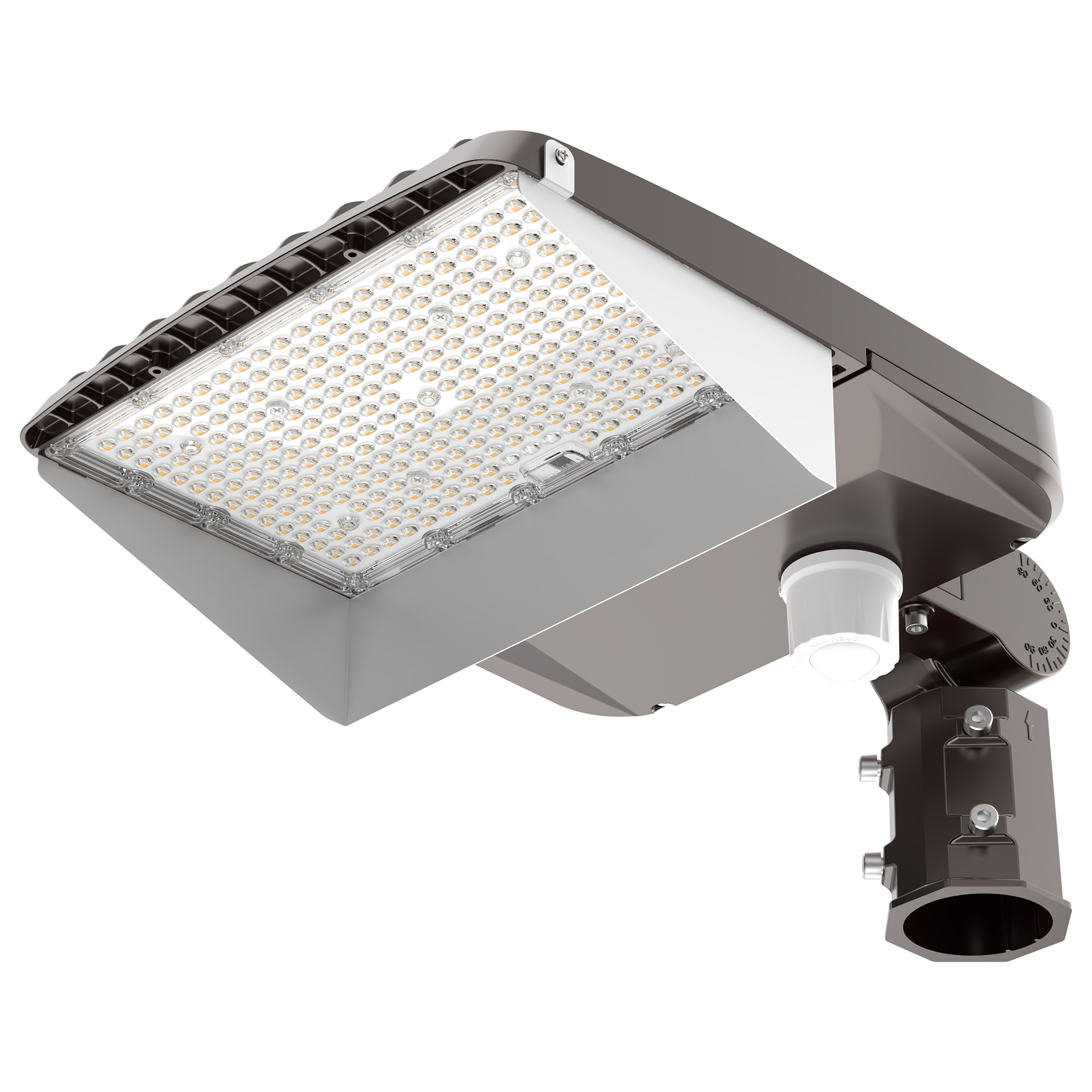
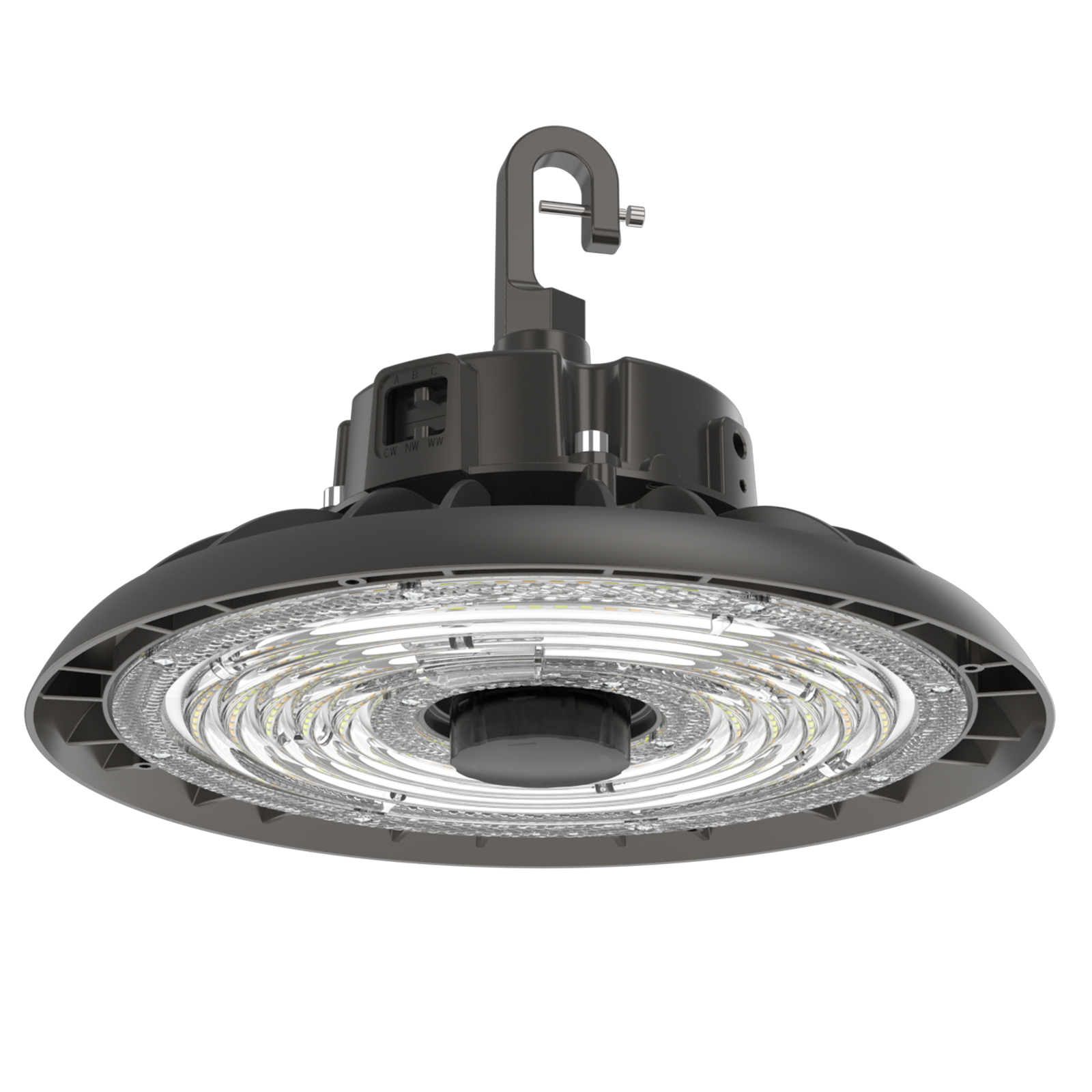
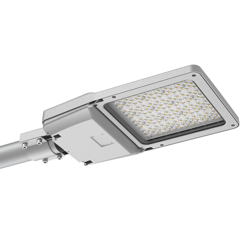
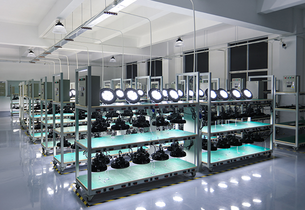
Found in 2008, Shenzhen Long Sun Optoelectronics Technology Co., Ltd has been focusing on industrial and commercial led lighting. With 14 years of experience in the research and development, manufacturing and marketing of LED product like LED high bay light, LED linear high bay, LED flood light, LED area light, LED street light, LED parking canopy and LED wall pack etc.
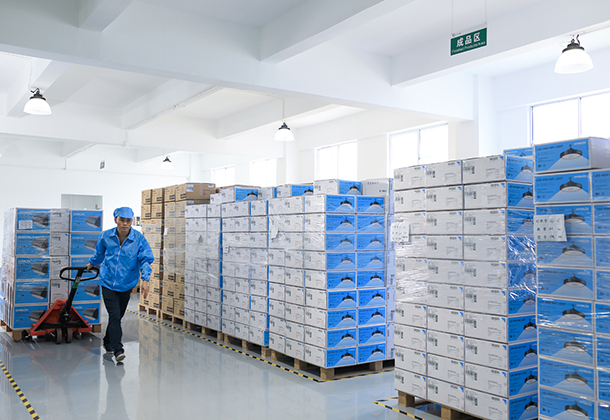
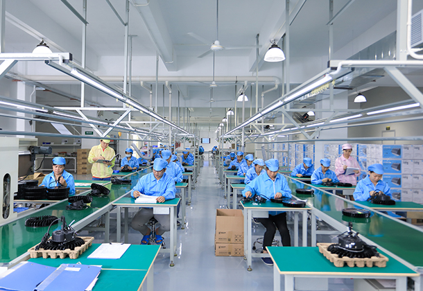
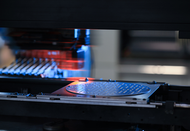
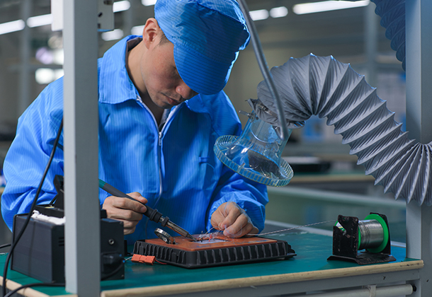
With over ten years' development, Long Sun has become one of the leading electronic manufacturers. There are over 10 R&D engineers and about 100 employees in the 4500 square meters Yang Guang Industrial Park, which is equipped with advanced machines such as Surface Mounting Machine, Integrating Sphere.....


 TEL: +86-0755-86369100
 E-MAIL: Sales010@longsun-led.com
 ADD: Room 304, Block B, Building 7, Shenzhen International Innovation Valley,
Dashi 1st Rd., Xili Community, Xili St., NanShan Dist.,ShenZhen
ADD: Room 304, Block B, Building 7, Shenzhen International Innovation Valley,
Dashi 1st Rd., Xili Community, Xili St., NanShan Dist.,ShenZhen
Copyright © Shenzhen Long Sun Optoelectronics Technology Co., Ltd 粤ICP备20036433号